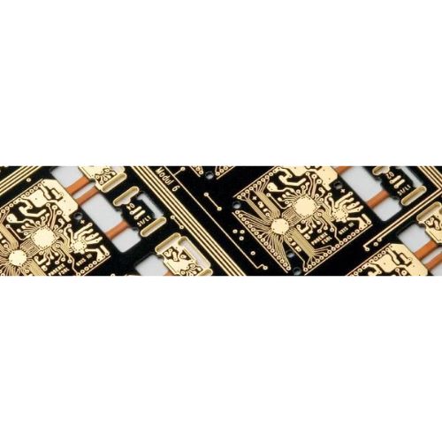
Due to its outstanding film characteristics EPIG deposition is very well suited to withstand the higher requirements of PCB designer concerning fine pattern ability and high performance regarding soldering and bonding process signal transfer in combination with complying newest RoHs and WEEE regulations.
Advantages
– Nickel free coating
– Thin and very uniform electroless deposition
– Suitable for (ultra) fine pitch layouts
– Ductile film compatible for flex PCB applications
– Dense and homogenous gold protection layer up to 0.3 μm feasible
– High solderjoint reliability (SJR) due to low void formation
– Excellent Al-, Au-, Cu-(Pd coated) and Ag-wire bondability


Reviews
There are no reviews yet.